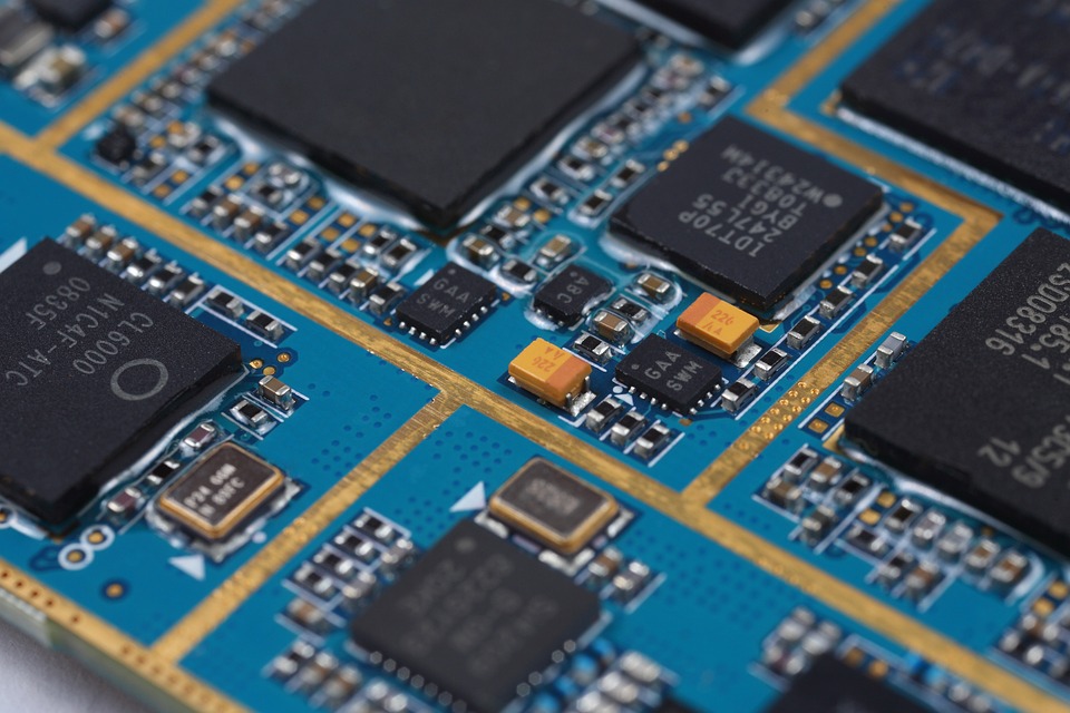
Designing for Space Efficiency: Strategies for Optimizing PCB Layout
As the demand for smaller, more powerful, and more affordable electronic devices continues to grow, PCB designers are facing new challenges in optimizing PCB layout for space efficiency. With the increasing complexity of modern electronics, designers must find ways to reduce the size of PCBs while maintaining their performance and reliability. In this article, we will explore the strategies and techniques for designing for space efficiency and optimizing PCB layout.
Why is Space Efficiency Important?
Space efficiency is crucial in PCB design for several reasons:
- Reduced cost: Smaller PCBs require less material, which can lead to significant cost savings.
- Increased density: By optimizing PCB layout, designers can fit more components on a smaller board, making it possible to create more complex systems in a smaller footprint.
- Improved reliability: By minimizing the distance between components and reducing the number of connections, designers can reduce the risk of faults and failures.
- Enhanced performance: Space-efficient PCBs can reduce signal delay, noise, and electromagnetic interference (EMI), leading to improved system performance.
Strategies for Optimizing PCB Layout
To optimize PCB layout for space efficiency, designers can use the following strategies:
1. Component Placement
Proper component placement is critical for optimizing PCB layout. Designers should:
- Place components in a way that minimizes the distance between them.
- Use component packages with a small footprint.
- Avoid placing components near the edges of the board.
- Use a consistent component placement scheme throughout the design.
2. Routing
Routing is a critical aspect of PCB design, and optimizing it can significantly improve space efficiency. Designers should:
- Use a routing strategy that minimizes the length of tracks.
- Avoid crossing tracks or components unnecessarily.
- Use vias and bridges to reduce the number of tracks.
- Minimize the number of layers required for routing.
3. Component Sizing
Component sizing is another important aspect of PCB design. Designers should:
- Use components with a small footprint.
- Avoid using components with a large profile.
- Use surface-mount components (SMTs) instead of through-hole components (THTs).
- Use lead-free components to reduce the overall size of the board.
4. Board Shape
The shape of the PCB board can also impact space efficiency. Designers should:
- Use a rectangular or square board shape to maximize space efficiency.
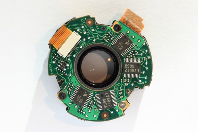
- Avoid using circular or irregular shapes that can waste space.
- Consider using a flexible PCB (FPC) or a flexible printed circuit (FPCB) for applications where a traditional rigid PCB is not feasible.
5. Stackup and Layer Count
The stackup and layer count of the PCB can also impact space efficiency. Designers should:
- Use a stackup with a small number of layers.
- Avoid using unnecessary layers or using layers that can be eliminated.
- Consider using a 2-layer or 4-layer PCB for simple designs.
Best Practices for Designing for Space Efficiency
In addition to the strategies outlined above, designers should also follow best practices for designing for space efficiency:
- Use design for manufacturability (DFM) principles to ensure that the PCB can be easily manufactured and assembled.
- Use design for test (DFT) principles to ensure that the PCB can be easily tested and validated.
- Use simulation tools to verify the performance of the PCB before it is manufactured.
- Use collaboration tools to share design data and feedback with stakeholders.
Conclusion
Designing for space efficiency is a critical aspect of PCB design. By optimizing PCB layout, designers can reduce the size of the board, minimize the number of components, and improve the overall performance and reliability of the system. By following the strategies and best practices outlined in this article, designers can create PCBs that are not only smaller and more efficient but also more reliable and cost-effective.
FAQs
Q: What are some common mistakes to avoid when designing for space efficiency?
A: Some common mistakes to avoid when designing for space efficiency include:
- Not considering the component package size.
- Not optimizing component placement.
- Not using simulation tools to verify the performance of the PCB.
- Not considering the impact of board shape and layer count on space efficiency.
Q: How can I ensure that my PCB design is manufacturable?
A: To ensure that your PCB design is manufacturable, you should:
- Use design for manufacturability (DFM) principles.
- Consider the manufacturing process and the tools used to manufacture the PCB.
- Use simulation tools to verify the performance of the PCB before it is manufactured.
- Collaborate with manufacturing stakeholders to ensure that the design meets their requirements.
Q: What are some tools and software available for designing for space efficiency?
A: Some tools and software available for designing for space efficiency include:
- Altium Designer.
- Autodesk Eagle.
- OrCAD.
- P-CAD.
- Siemens EDA.
Q: How can I measure the space efficiency of my PCB design?
A: To measure the space efficiency of your PCB design, you can use metrics such as:
- Component density.
- Track density.
- Layer count.
- Board size.
- Component size.
Q: What are some best practices for collaborating with stakeholders when designing for space efficiency?
A: Some best practices for collaborating with stakeholders when designing for space efficiency include:
- Using collaboration tools to share design data and feedback.
- Establishing clear communication channels with stakeholders.
- Using project management tools to track progress and milestones.
- Conducting regular design reviews and feedback sessions.

